Many PCB designers get to a point where they need to put some artwork on a board they're designing. Some time ago I had to do just that and it appeared that there is no trivial solution in kicad.
In this post I'm going to show you how to make pretty logos in pcbnew.
Kicad offers a simple program called bitmap2component which vectorizes any bitmap image and makes an eeschema or pcbnew module. We won't be dealing with eeschema here, since this isn't very interesting, but getting a pcbnew module is very useful. Unfortunately, the tool offers very little functionality and in most cases it won't be enough for most things (as of the version from 2012-oct-18).
Making silkscreen artwork
The program's interface essentially looks like in the picture below and it's basic workflow is: load a file, export as component. Not really exciting.

It requires that your artwork be white and the background black, but it has a negative option and a settable threshold value if you don't want to do much preprocessing.
After loading the generated file into pcbnew, you'll see that it's as basic as it can be. Just a shape on the silkscreen layer. The program assumes arbitrary input resolution of 300ppi, so a 300 by 300 image will give a 1" by 1" logo on the board.
Now this is the first problem I came across. If the artwork is complicated, the vectorizer will not give nice sharp edges. This is rather standard behavior of vectorizers - they always need high resolution bitmaps to deal with details, even if the resolution seems enough.
Here's an example of how the vectorization is done with the same image but different resolutions.
This is the input image in 2 different resolutions:

You can see that the scaled-down version of the image doesn't lack any shape details. Below are the results of conversion (scaled to the same size)

As you can see the lower-resolution image was converted to a shape with much more rounded and smooth corners and this is what you usually don't want.
So what I want to do is feed the vectorizer with much higher resolution image to make sure the output shape is correct and then scale the module down.
For this purpose I wrote a very simple script which preprocesses the module by scaling it by a constant factor and changing its name (as you can't do that in the current version of bitmap2component either):
|
1 2 3 4 5 6 |
infile=$1 outfile=$2 name=$3 scale=$4 awk '/Dl|T0|T1/{$2=int($2/'$scale'); $3=int($3/'$scale')} //{print $0}' "$infile" | sed -e 's/LOGO/'$name'/g' > "$outfile" |
This scales the module by dividing both dimensions of every point by a number passed as parameter. It also sets a new module name (instead of "LOGO"). The usage is simple:
|
1 |
./scale.sh in_file.mod out_file.mod module_name scale |
For example, to simply make a 1cm by 1cm image, prepare a bitmap file of resolution 1180x1180 (since 1cm is 118 pixels), convert it to module and then run the script with scale set to 10.
Since the module file generated by the vectorizer contains information about original image's dimensions, the script could actually be extended to take that into account and generate a module of any physical dimensions. But I won't do that, since I generate such components only on occasion.
Generating prettier artwork
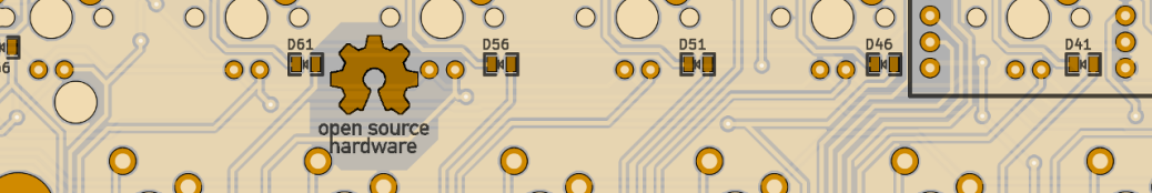
Artwork on PCBs doesn't have to be limited to silkscreen. In fact it can be much better-looking without silkscreen at all. One idea is to uncover a part of the soldermask to reveal the copper underneath. Since the PCB fabs usually offer rather high soldermask resolution, sometimes better than that of silkscreen, the image "printed" this way can look very good, and it actually does in reality. It looks even better when the board is gold-plated, but this is becoming a standard these days.
In order to generate this kind of effect we need the module to have 2 layers. The soldermask expansion to reveal bare copper and the actual copper layer. Since PCB fabs can't avoid some offset between layers, making these 2 layers exactly the same isn't a good idea, since just a 0.1mm shift will probably look bad. So for a start we need a logo and it's larger (dilated) version. This can be easily prepared in any raster graphics program, like The Gimp.


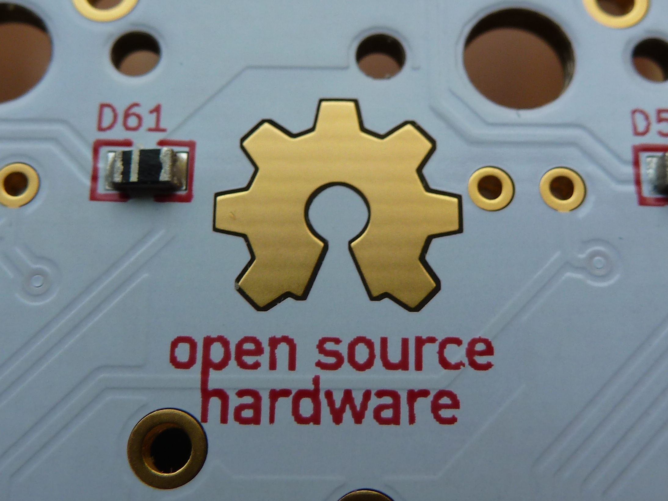
For this article, let's take the Open Source Hardware logo. On the left is a preprocessed black and white logo. I used The Gimp's Dilate filter a couple of times to generate the larger soldermask expansion. When using this filter, it's important to work on a real black and white image, without nice anti-aliased edges. The soldermask expansion is shown on the right. Then I converted both graphics (remember to keep the image sizes the same) to modules using the vectorizer.
Now two things remain to be done. The layers have to be changed accordingly and the two modules have to be merged into one.
Some documentation concerning kicad's file formats is available on the internet, but to put it simple: we care only for one type of lines in this file - the ones which start from DP. These lines define polygons and contain layer information. The eighth field is the layer number. There may be some problems finding the numbers for particular layers on the Web, so my small empiric research showed that copper is 15 and soldermask is 23. I put together this little script to change layer numbers and join two modules together:
|
1 2 3 4 5 |
mod_copper=$1 mod_mask=$2 output=$3 (awk '/EndMODULE/ {n=1} /DP/ {$8=15} !n {print $0}' "$mod_copper" && awk '/DP/ {y=1} /DP/ {$8=23} y {print $0}' "$mod_mask") > "$output" |
Usage is, again, simple:
|
1 |
./join.sh copper_module.mod mask_module.mod output.mod |

After that, you will most probably need to scale the generated module and set a sensible name with the previous script. The result is shown on the right. The solution generates the result for the top layer. For the bottom one it's enough to flip the module in pcbnew, but the actual polygons will not be flipped, so you'll need to flip them manually before converting to modules. An alternative option is to add this functionality to the script, of course.
Obviously there are a lot of enhancements to be done. The script could automatically generate a dilated version of the copper module, since the dilation algorithm is rather simple for polygons. Also silkscreen layer could be attached to the output module to form a single module with everything you need to have a pretty logo. But this you can quite as well do yourself;).
Results and remarks
Here's an example how a connection of these two techniques looks in reality. This is a standard FR4 board with black matte soldermask and ENIG gold-plating:
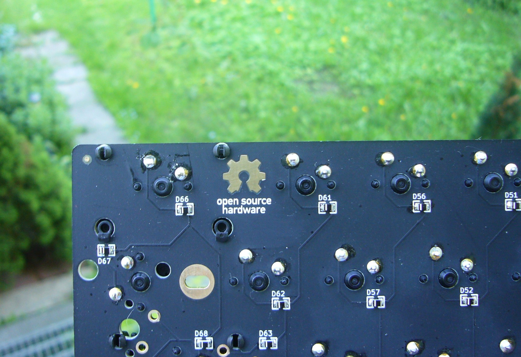
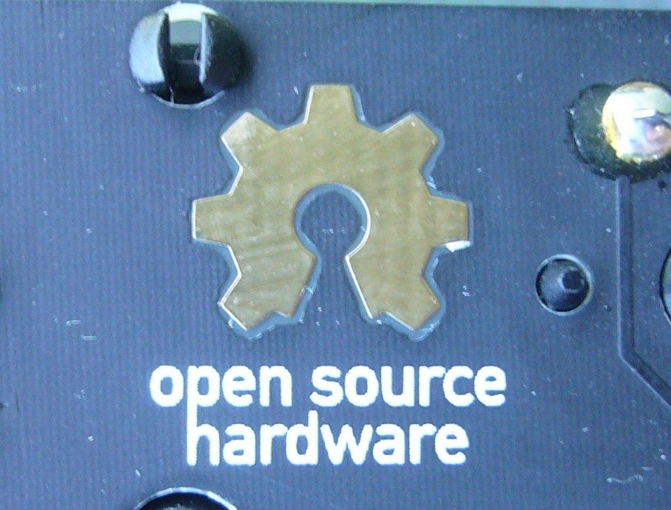 The closeup reveals some imperfections of the production process, though. You can see that the soldermask cutout is shifted a bit and its shape is simplified a lot compared to the project. Fortunately, it doesn't look that bad from a sensible distance.
And that's all. This is how you do artwork in pcbnew. I hope it was useful and informative in any way. If you have any new ideas or enhancements to propose, leave them in the comments section!
Update
Here's a closeup of the same logo on the GH60 rev. B board with glossy white soldermask:
Hello,
Can you please contact me. Looking for Gerber file for a mini keyboard
Thanks
Hi,
please check out the GH60 project! http://blog.komar.be/projects/gh60-programmable-keyboard/
The newest version is available on github. Final PCB revision gerbers coming soon too.
Thank you for the scaling script. I scoured the web looking for a solution to produce good quality, small LOGOs for kicad and this is the best and most clever approach I've seen (that's a clever little script). Nice work!
Thanks, Devin.
It's good to know it's useful!
Thanks very much for the post, it worked brilliantly.
Although I did run into one problem, pcbnew doesn't seem to be able to properly flip the module onto the backside. It flips the associated text (refs and values) but not the module itself. Unfortunately I didn't catch this error until after the boards were printed... Any thoughts on why this might be happening? I could easily make a new module with the original image flipped, but I'd rather have the program work properly.
Thanks
jay
I know it doesn't work that way, I'm not sure it's a bug or a feature. So far the only way to put artwork on either side I know of is to prepare 2 module versions, 1 flipped.
It might be because nobody assumed there would be any copper layers in modules, since you can't even add them in the module editor, so it makes sense it doesn't work correctly. All in all, the solution here is just a hack.
Thanks for the informative post.
How can I make a bitmap module of a logo show up on next to the title block when printing?
I'd think one would be able to move the module to layer Drawings, and it would print, but it does not.
Thanks for any help you may be able to provide.
I can put a logo in schematics ok....
Clyde
Hi Clyde,
after using bitmap2component I recommend the following script to change the layer to drawings, scale and rename a module:
scale=10 # example only
name=testmodule # example only
awk '/Dl|T0|T1/{$2=int($2/'$scale'); $3=int($3/'$scale')} /DP/ {$8=24} // {print}' input.mod | sed "s/LOGO/$name/g" > result.mod
The number 24 in this script is the layer number for Drawings.
You can check the layer numbers by saving anything in pcbnew in the new kicad_pcb format. Somewhere at the beginning of the file is the list of layers with their numbers.
And when printing, don't forget to select the Drawings layer;)
Best regards,
Michał
Thanks.
Unfortunately I have not coverted over my module library to the new format yet. I started to do it and had a bad experience nearly spoiling my entire library.
Any thoughts on the old format would be helpful.
Clyde
The script works on the old .mod files.
The new format is only helpful if you want to check the layer numbers easily. As far as I know the old modules work with the new format as well.
Hi,
I was looking for some information on PCB Assembly today when I came across your awesome website.
Great stuff!
Actually, I just put together an infographic about "Assembly Methods for Printed Circuit Boards”. As someone that who's on Electronics, I thought you might get a kick out of it.
Let me know if you want to check it out.
Cheers,
Algen
Thanks Algen,
why don't you link it here or use pingback so that we can check it out?
Best regards,
Michał
hi mate i run cicada on a mac what is the best way for me to do this, edit the files?
Hi,
can you elaborate? What do you want to do?
im trying to do a logo with a new mod in os x i have created the copper that was fine, but if i change to f.mask i get an error in kicad, any suggestion,
kicad file
Hi,
I'm not sure I can reproduce that. Where do you change to f.mask? And what's the error?
hi komar,
thanks for this,now i am studying about the PCB board it is very useful for me i got some idea about your blog
thank you